

MAX120是Maxim美信半导体公司的一款数据转换器和采样-保持电路产品,MAX120是500ksps、12位ADC,带有采样/保持和电压基准,本站介绍了MAX120的封装应用图解、特点和优点、功能等,并给出了与MAX120相关的Maxim元器件型号供参考。
MAX120 - 500ksps、12位ADC,带有采样/保持和电压基准 - 数据转换器和采样-保持电路 - Maxim美信半导体高性能芯片品质 - 美信半导体
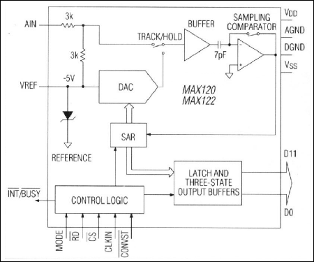
The MAX120/MAX122 complete, BiCMOS, sampling 12-bitanalog-to-digital converters (ADCs) combine an on-chiptrack/hold (T/H) and a low-drift voltage reference with fastconversion speeds and low-power consumption. The T/H’s350ns acquisition time combined with the MAX120’s 1.6µsconversion time results in throughput rates as high as 500ksamples per second (ksps). Throughput rates of 333kspsare possible with the 2.6μs conversion time of the MAX122.
The MAX120/MAX122 accept analog input voltages from-5V to +5V. The only external components needed aredecoupling capacitors for the power-supply and referencevoltages. The MAX120 operates with clocks in the0.1MHz to 8MHz frequency range. The MAX122 accepts0.1MHz to 5MHz clock frequencies.
The MAX120/MAX122 employ a standard microprocessor(µP) interface. Three-state data outputs are configuredto operate with 12-bit data buses. Data-access and bus-releasetiming specifications are compatible with mostpopular µPs without resorting to wait states. In addition,the MAX120/MAX122 can interface directly to a first-in,first-out (FIFO) buffer, virtually eliminating µP interruptoverhead. All logic inputs and outputs are TTL/CMOScompatible. For applications requiring a serial interface,refer to the MAX121.