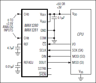

MAX1280B是Maxim美信半导体公司的一款美信芯片产品,MAX1280B是400ksps/300ksps、单电源、低功耗、8通道、串行12位ADC,内置电压基准,本站介绍了MAX1280B的封装应用图解、特点和优点、功能等,并给出了与MAX1280B相关的Maxim元器件型号供参考。
MAX1280B - 400ksps/300ksps、单电源、低功耗、8通道、串行12位ADC,内置电压基准 - 美信芯片 - Maxim美信半导体高性能芯片品质 - 美信半导体
The MAX1280/MAX1281 12-bit ADCs combine an 8-channel analog-input multiplexer, high-bandwidth track/hold, and serial interface with high conversion speed and low power consumption. The MAX1280 operates from a single +4.5V to +5.5V supply; the MAX1281 operates from a single +2.7V to +3.6V supply. Both devices' analog inputs are software configurable for unipolar/bipolar and single-ended/pseudo-differential operation.
The 4-wire serial interface connects directly to SPI™/QSPI™/MICROWIRE™ devices without external logic. A serial strobe output allows direct connection to TMS320-family digital signal processors. The MAX1280/MAX1281 use an external serial-interface clock to perform successive-approximation analog-to-digital conversions. Both parts feature an internal +2.5V reference and a reference-buffer amplifier with a ±1.5% voltage-adjustment range. An external reference with a 1V to VDD1 range may also be used.
The MAX1280/MAX1281 provide a hard-wired active-low SHDN pin and four software-selectable power modes (normal operation, reduced power, fast power-down, and full power-down). These devices can be programmed to automatically shut down at the end of a conversion or to operate with reduced power. When using the power-down modes, accessing the serial interface automatically powers up the devices, and the quick turn-on time allows them to be powered down between all conversions. This technique can cut supply current to under 100µA at reduced sampling rates.
The MAX1280/MAX1281 are available in 20-pin TSSOP packages. These devices are higher-speed versions of the MAX146/MAX147 (for more information, see the respective data sheet).


