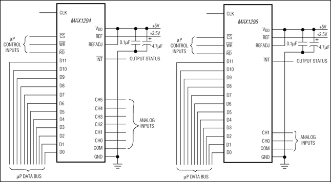

MAX1296是Maxim美信半导体公司的一款数据转换器和采样-保持电路产品,MAX1296是420ksps、+5V、6/2通道、12位ADC,带有+2.5V电压基准及并行接口,本站介绍了MAX1296的封装应用图解、特点和优点、功能等,并给出了与MAX1296相关的Maxim元器件型号供参考。
MAX1296 - 420ksps、+5V、6/2通道、12位ADC,带有+2.5V电压基准及并行接口 - 数据转换器和采样-保持电路 - 尺寸最小的低功耗、并行输出、12位ADC - 美信半导体
The MAX1294/MAX1296 low-power, 12-bit analog-to-digital converters (ADCs) feature a successive-approximation ADC, automatic power-down, fast wake-up (2µs), an on-chip clock, +2.5V internal reference, and a high-speed 12-bit parallel interface. They operate with a single +5V analog supply.
Power consumption is only 10mW at the maximum sampling rate of 420ksps. Two software-selectable power-down modes enable the MAX1294/MAX1296 to be shut down between conversions; accessing the parallel interface returns them to normal operation. Powering down between conversions can reduce supply below 10µA at lower sampling rates.
Both devices offer software-configurable analog inputs for unipolar/bipolar and single-ended/pseudo-differential operation. In single-ended mode, the MAX1294 has six input channels and the MAX1296 has two (three input channels and one input channel, respectively, when in pseudo-differential mode).
Excellent dynamic performance and low power, combined with ease of use and small package size, make these converters ideal for battery-powered and data-acquisition applications or for other circuits with demanding power-consumption and space requirements.
The MAX1294/MAX1296 tri-states active-low INT when active-low CS goes high. Refer to MAX1266/MAX1268 if tri-stating active-low INT is not desired.
The MAX1294 is offered in a 28-pin QSOP package, while the MAX1296 is available in a 24-pin QSOP. For pin-compatible +3V, 12-bit versions, see the MAX1295/MAX1297.


