
MAX1421是Maxim美信半导体公司的一款数据转换器和采样-保持电路产品,MAX1421是12位、40Msps、3.3V、低功耗ADC,内置电压基准,本站介绍了MAX1421的封装应用图解、特点和优点、功能等,并给出了与MAX1421相关的Maxim元器件型号供参考。
MAX1421 - 12位、40Msps、3.3V、低功耗ADC,内置电压基准 - 数据转换器和采样-保持电路 - Maxim美信半导体高性能芯片品质 - 美信半导体
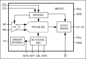
The MAX1421 is a 3.3V, 12-bit analog-to-digital converter(ADC), featuring a fully-differential input,pipelined, 12-stage ADC architecture with widebandtrack-and-hold (T/H) and digital error correction incorporatinga fully-differential signal path. The MAX1421 isoptimized for low-power, high-dynamic performanceapplications in imaging and digital communications.The converter operates from a single 3.3V supply, consumingonly 188mW while delivering a typical signal-to-noiseratio (SNR) of 66dB at an input frequency of15MHz and a sampling frequency of 40Msps. The fully-differentialinput stage has a small signal -3dB bandwidthof 400MHz and may be operated withsingle-ended inputs.
An internal 2.048V precision bandgap reference setsthe full-scale range of the ADC. A flexible referencestructure accommodates an internal or externallyapplied buffered or unbuffered reference for applicationsrequiring increased accuracy or a different inputvoltage range.
In addition to low operating power, the MAX1421 featurestwo power-down modes, a reference power-downand a shutdown mode. In reference power-down, theinternal bandgap reference is deactivated, resulting ina typical 2mA supply current reduction. For idle periods,a full shutdown mode is available to maximizepower savings.
The MAX1421 provides parallel, offset binary, CMOS-compatiblethree-state outputs.
The MAX1421 is available in a 7mm x 7mm, 48-pinTQFP package, and is specified over the commercial(0°C to +70°C) and the extended industrial (-40°C to+85°C) temperature ranges.
Pin-compatible higher- and lower-speed versions of theMAX1421 are also available. Please refer to theMAX1420 data sheet for a frequency of 60Msps andthe MAX1422 data sheet for a frequency of 20Msps.


