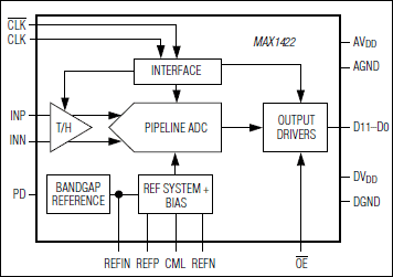

MAX1422是Maxim美信半导体公司的一款数据转换器和采样-保持电路产品,MAX1422是12位、20Msps、+3.3V、低功耗ADC,内置电压基准,本站介绍了MAX1422的封装应用图解、特点和优点、功能等,并给出了与MAX1422相关的Maxim元器件型号供参考。
MAX1422 - 12位、20Msps、+3.3V、低功耗ADC,内置电压基准 - 数据转换器和采样-保持电路 - Maxim美信半导体高性能芯片品质 - 美信半导体
The MAX1422 3.3V, 12-bit analog-to-digital converter(ADC) features a fully differential input, pipelined, 12-stage ADC architecture with wideband track-and-hold(T/H) and digital error correction incorporating a fully-differentialsignal path. The MAX1422 is optimized for lowpower,high dynamic performance applications inimaging and digital communications. The converteroperates from a single 3.3V supply, consuming only137mW while delivering a 67dB (typ) signal-to-noiseratio (SNR) at a 5MHz input frequency and a 20Mspssampling frequency. The fully-differential input stagehas a small signal -3dB bandwidth of 400MHz and maybe operated with single-ended inputs.
An internal 2.048V precision bandgap reference setsthe ADCs full-scale range. A flexible reference structureaccommodates an internally or externally appliedbuffered or unbuffered reference for applicationsrequiring increased accuracy or a different input voltagerange.
In addition to low operating power, the MAX1422 featurestwo power-down modes, a reference power-down, and ashutdown mode. In reference power-down, the internalbandgap reference is deactivated, resulting in a 2mA(typ) supply current reduction. For idle periods, a fullshutdown mode is available to maximize power savings.
The MAX1422 provides parallel, offset binary, CMOS-compatiblethree-state outputs.
The MAX1422 is available in a 7mm x 7mm x 1.4mm,48-pin TQFP package and is specified over the commercial(0°C to +70°C) and extended industrial (-40°Cto +85°C) temperature ranges.
Pin-compatible higher-speed versions of the MAX1422are also available. Please refer to the MAX1421 datasheet for 40Msps and the MAX1420 data sheet for60Msps.


