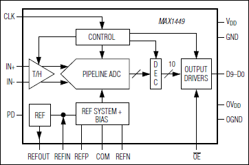

MAX1449是Maxim美信半导体公司的一款数据转换器和采样-保持电路产品,MAX1449是10位、105Msps、单路+3.3V、低功耗ADC,内置电压基准,本站介绍了MAX1449的封装应用图解、特点和优点、功能等,并给出了与MAX1449相关的Maxim元器件型号供参考。
MAX1449 - 10位、105Msps、单路+3.3V、低功耗ADC,内置电压基准 - 数据转换器和采样-保持电路 - 3.3V、10位、105Msps ADC,具有70dBc SFDR - 美信半导体
The MAX1449 3.3V, 10-bit analog-to-digital converter (ADC) features a fully differential input, a pipelined 10-stage ADC architecture with wideband track-and-hold (T/H), and digital error correction incorporating a fully differential signal path. The ADC is optimized for lowpower, high-dynamic performance in imaging and digital communications applications. The converter operates from a single 2.7V to 3.6V supply, consuming only 186mW while delivering a 58.5dB (typ) signal-to-noise ratio (SNR) at a 20MHz input frequency. The fully differential input stage has a -3dB 400MHz bandwidth andmay be operated with single-ended inputs. In addition to low operating power, the MAX1449 features a 5µA power-down mode for idle periods.
An internal 2.048V precision bandgap reference is used to set the ADC's full-scale range. A flexible reference structure allows the user to supply a buffered, direct, or externally derived reference for applications requiring increased accuracy or a different input voltage range.
See a parametric table of the complete family of pin-compatible, 10-bit high-speed ADCs.
The MAX1449 has parallel, offset binary, CMOS-compatible, three-state outputs that can be operated from 1.7V to 3.6V to allow flexible interfacing. The device is available in a 5mm x 5mm 32-pin TQFP package and is specified over the extended industrial (-40°C to +85°C) temperature range.


