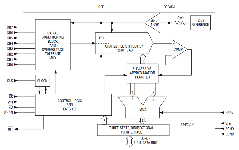

MAX197是Maxim美信半导体公司的一款数据转换器和采样-保持电路产品,MAX197是多量程(±10V, ±5V, +10V, +5V)、单+5V、12位数DAS,8+4总线接口,本站介绍了MAX197的封装应用图解、特点和优点、功能等,并给出了与MAX197相关的Maxim元器件型号供参考。
MAX197 - 多量程(±10V, ±5V, +10V, +5V)、单+5V、12位数DAS,8+4总线接口 - 数据转换器和采样-保持电路 - ±17V故障保护ADC,可通过软件选择输入量程 - 美信半导体
The MAX197 multi-range, 12-bit data-acquisition system (DAS) requires only a single +5V supply for operation, yet accepts signals at its analog inputs that may span both above the power-supply rail and below ground. This system provides 8 analog input channels that are independently software programmable for a variety of ranges: ±10V, ±5V, 0V to +10V, or 0V to +5V. This increases effective dynamic range to 14 bits, and provides the user flexibility to interface 4mA-to-20mA, ±12V, and ±15V powered sensors to a single +5V system. In addition, the converter is overvoltage tolerant to ±16.5V; a fault condition on any channel does not affect the conversion result of the selected channel. Other features include a 5MHz bandwidth track/hold, a 100ksps throughput rate, software-selectable internal or external clock and acquisition, 8+4 parallel interface, and an internal 4.096V or an external reference.
A hardware active-low SHDN pin and two programmable power-down modes (STBYPD, FULLPD) are provided for low-current shutdown between conversions. In STBYPD mode, the reference buffer remains active, eliminating start-up delays.
The MAX197 employs a standard microprocessor (µP) interface. A three-state data I/O port is configured to operate with 8-bit data buses, and data-access and bus-release timing specifications are compatible with most popular µPs. All logic inputs and outputs are TTL/CMOS compatible.
The MAX197 is available in 28-pin DIP, wide SO, SSOP, and ceramic SB packages.
For a different combination of ranges (±4V, ±2V, 0V to 4V, 0V to 2V), refer to the MAX199 data sheet. For 12-bit bus interface, refer to the MAX196 and MAX198 data sheets.


