
MAX501是Maxim美信半导体公司的一款数据转换器和采样-保持电路产品,MAX501是电压输出、12位乘法DAC,本站介绍了MAX501的封装应用图解、特点和优点、功能等,并给出了与MAX501相关的Maxim元器件型号供参考。
MAX501 - 电压输出、12位乘法DAC - 数据转换器和采样-保持电路 - Maxim美信半导体高性能芯片品质 - 美信半导体
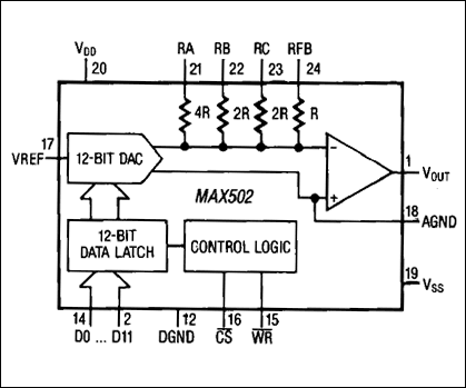
The MAX501/MAX502 are 12-bit, 4-quadrant, voltage-output, multiplying digital-to-analog converters (DACs) with an output amplifier. Thin-film resistors, laser trimmed at the wafer level, maintain accuracy over the full operating temperature range.
The MAX501/MAX502 have buffered latches that are easily interfaced with microprocessors. Data is transferred into the input register in either a right-justified 8 + 4-bit format (MAX501) or with a 12-bit-wide data path (MAX502). In the MAX501, an active-low LDAC signal transfers data from the input register to the DAC register. In the MAX502, the input registers are controlled by standard active-low CHIP SELECT (active-low CS) and active-low WRITE (active-low WR) signals. For stand-alone operation, the active-low CS and active-low WR inputs are grounded, making all latches transparent. All logic inputs are level triggered and compatible with TTL and +5V CMOS logic levels. The internally compensated, low-input offset-voltage output amplifier provides an output voltage from +10V to -10V while sourcing and sinking up to 5mA.


