
MAX512是Maxim美信半导体公司的一款数据转换器和采样-保持电路产品,MAX512是低成本、3通道、8位、电压输出DAC,串行接口,本站介绍了MAX512的封装应用图解、特点和优点、功能等,并给出了与MAX512相关的Maxim元器件型号供参考。
MAX512 - 低成本、3通道、8位、电压输出DAC,串行接口 - 数据转换器和采样-保持电路 - 三通道、串行、电压输出DAC,SO封装 - 美信半导体
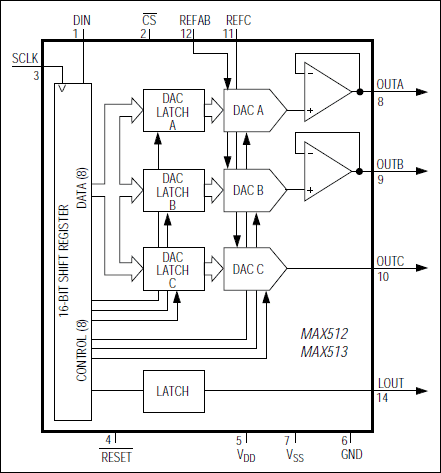
The MAX512/MAX513 contain three 8-bit, voltage-output digital-to-analog converters (DAC A, DAC B, and DAC C). Output buffer amplifiers for DACs A and B provide voltage outputs while reducing external component count. The output buffer for DAC A can source or sink 5mA to within 0.5V of VDD or VSS. The buffer for DAC B can source or sink 0.5mA to within 0.5V of VDD or VSS. DAC C is unbuffered, providing a third voltage output with increased accuracy. The MAX512 operates with a single +5V ±10% supply, and the MAX513 operates with a +2.7V to +3.6V supply. Both devices can also operate with split supplies.
The 3-wire serial interface has a maximum operating frequency of 5MHz and is compatible with SPI™, QSPI™, and Microwire™. The serial input shift register is 16 bits long and consists of 8 bits of DAC input data and 8 bits for DAC selection and shutdown. DAC registers can be loaded independently or in parallel at the positive edge of CS. A latched logic output is also available for auxiliary control.
Ultra-low power consumption and small packages (14-pin DIP/SO) make the MAX512/MAX513 ideal for portable and battery-powered applications. Supply current is only 1mA, dropping to less than 1µA in shutdown. Any of the three DACs can be independently shut down. In shutdown mode, the DAC's R-2R ladder network is disconnected from the reference input, minimizing system power consumption.


