
MAX537是Maxim美信半导体公司的一款数据转换器和采样-保持电路产品,MAX537是校准型、四路、12位、电压输出DAC,串行接口,本站介绍了MAX537的封装应用图解、特点和优点、功能等,并给出了与MAX537相关的Maxim元器件型号供参考。
MAX537 - 校准型、四路、12位、电压输出DAC,串行接口 - 数据转换器和采样-保持电路 - 四通道、串行、电压输出DAC,SO封装 - 美信半导体
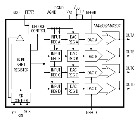
The MAX536/MAX537 combine four 12-bit, voltage-output digital-to-analog converters (DACs) and four precision output amplifiers in a space-saving 16-pin package. Offset, gain, and linearity are factory calibrated to provide the MAX536's ±1 LSB total unadjusted error. The MAX537 operates with ±5V supplies, while the MAX536 uses -5V and +10.8V to +13.2V supplies.
Each DAC has a double-buffered input, organized as an input register followed by a DAC register. A 16-bit serial word is used to load data into each input/DAC register. The serial interface is compatible with either SPI/QSPI™ or MICROWIRE™, and allows the input and DAC registers to be updated independently or simultaneously with a single software command. The DAC registers can be simultaneously updated with a hardware active-low LDAC pin. All logic inputs are TTL/CMOS compatible.


